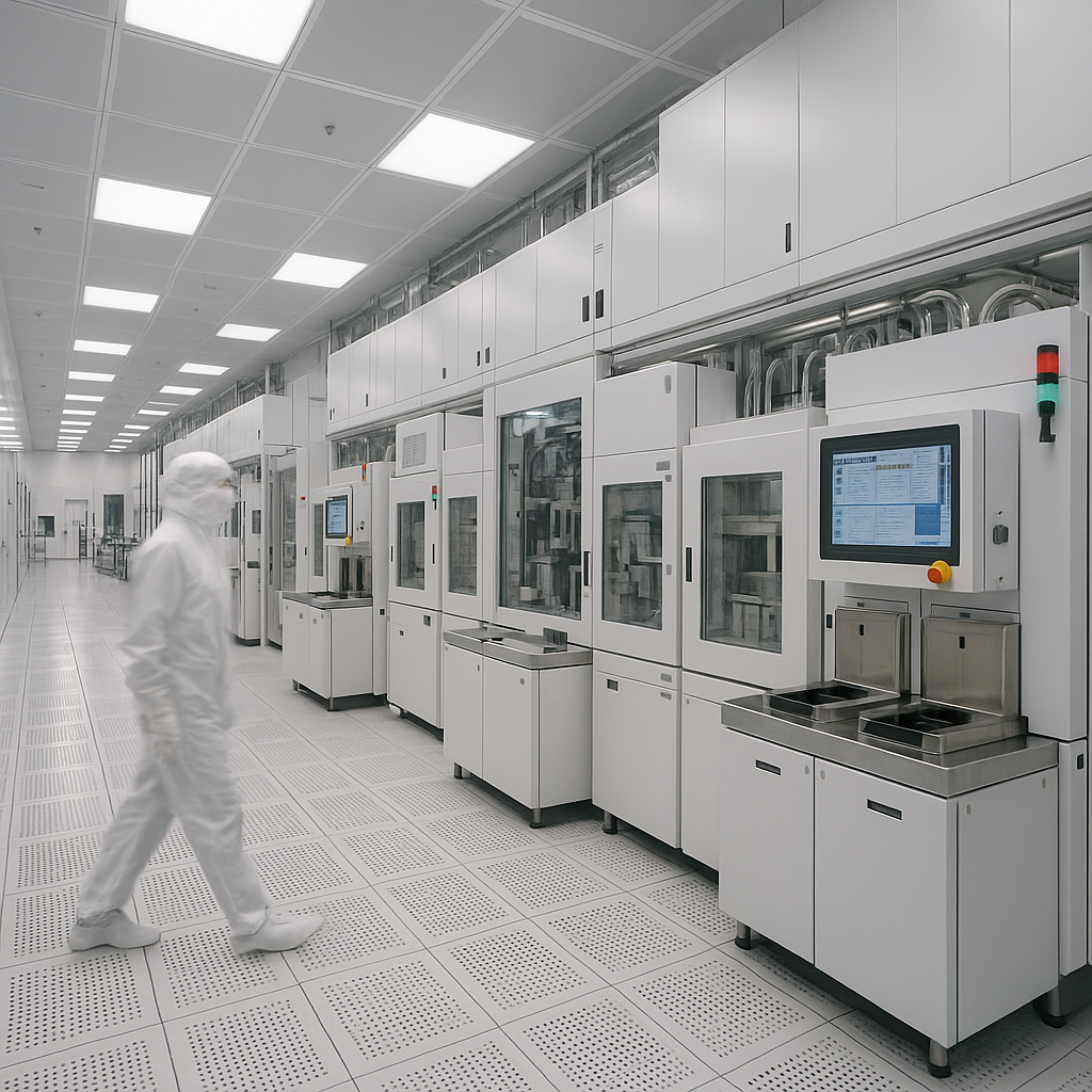
Our Manufacturing Approach

Why MONK?

MONK represents focus, discipline, precision, and mastery the same qualities required to manufacture semiconductors at nanometer scale.

01

Focus on What Matters

Advanced nodes are not required for most real-world applications. Over 60% of global chips are still manufactured on mature nodes.

MONK focuses on nodes that:

  • Are widely used
  • Are supply-constrained
  • Have long product lifecycles
  • Are critical for national and industrial infrastructure

02

India-Centric Manufacturing

MONK is built with the mission of strengthening India’s semiconductor self-reliance while meeting global standards.

03

Discipline Over Hype

Semiconductor manufacturing demands:

  • Repeatability
  • Process discipline
  • Yield learning
  • Long-term stability

MONK follows a manufacturing-first mindset rather than hype-driven scaling.

04

Partner, Not Just a Foundry

We don’t just manufacture wafers, we support customers with:

  • Process customization
  • Technology enablement
  • Long-term supply assurance
  • Transparent collaboration

Value-Focused

Technology Nodes

MONK specializes in mature technology nodes, 350 nm, 180 nm, and 130 nm that power over 60% of global semiconductor production.

350 nm
  • Power management ICs
  • Industrial controllers
  • Sensors
180 nm
  • Analog & mixed-signal ICs
  • Display drivers
  • Automotive electronics
  • IoT and industrial applications
130 nm
  • High-performance analog
  • RF and mixed-signal
  • Secure and defense electronics
  • Embedded non-volatile memory integration
No alt text
Fab 2.0 Semiconductor Manufacturing

India’s Fab 2.0 initiative delivers legacy node fabrication with a roadmap to advanced research, supported by global-grade equipment and state-backed incentives.

No alt text
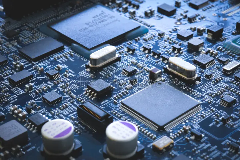
Products & Semiconductor Technology

A growing portfolio of CMOS image sensors, RISC-V IP, standard cell libraries, and advanced node research platforms for next-generation silicon.
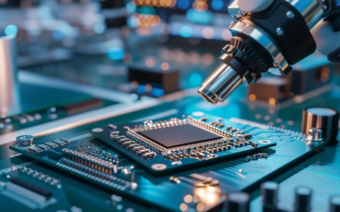
No alt text
Design Services (EDA & PDK)

End-to-end chip design enablement including PDK development, RTL-to-GDSII flows, and open-source EDA integration for rapid tape-outs.

No alt text
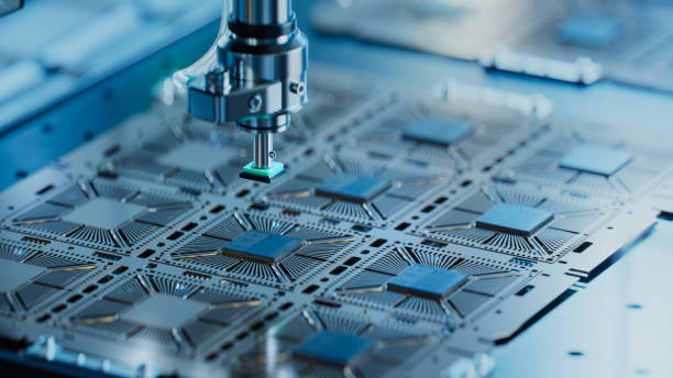
Manufacturing & Production Services

Comprehensive manufacturing support covering wafer fabrication, MPW shuttles, device characterization, inspection, and packaging services.