

Quick Services
Overview
Monk9 Tech provides end-to-end semiconductor design enablement through PDK development and EDA services. Our design stack supports legacy nodes and advanced research platforms, enabling reliable tape-outs for industry, academia, and startups.
EDA & Design Services
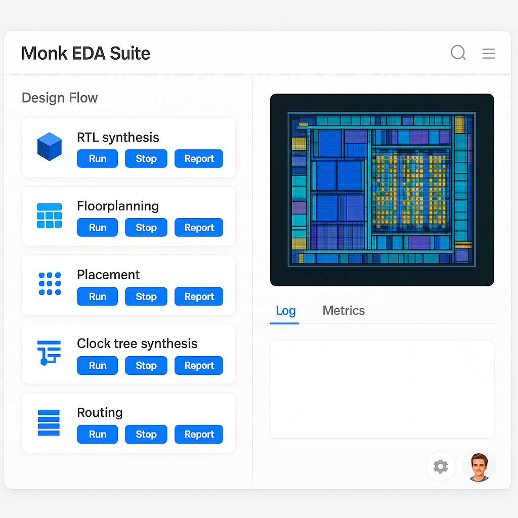
Our EDA services cover the complete digital design flow from RTL to sign-off.
Core EDA Capabilities
- RTL design
- Floorplanning & Place-and-Route (PnR)
- Timing closure
- LVS / DRC sign-off
- DFT insertion
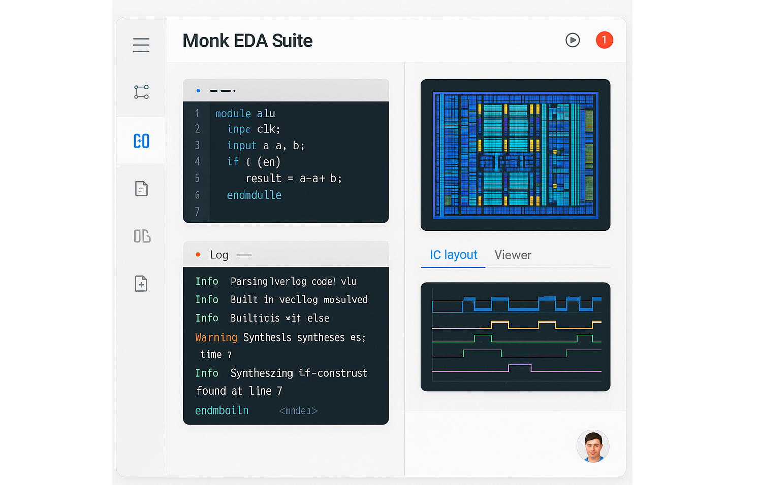
Design Tools & Platform
- ChipMonk Dashboard integration (Monk9 EDA GUI)
PDK Development Services
Monk9 Tech develops semi-open and academic Process Design Kits (PDKs) to accelerate chip design and research workflows.
Supported Nodes
- 350 nm
- 180 nm
- 3 nm (research)
Additional Kits
- Packaging Design Kits